A quick guide on how to make a PCB footprint
Creating footprints for electronic components on printed circuit boards is a crucial part of the electronic device design process. The overall functionality and reliability of the PCB depends on their quality.
Maintaining a balanced PCB footprint size is essential. Overly large footprints occupy excessive space on the board and limit routing possibilities. Too small pads decrease soldering reliability and the overall reliability of the PCB. It’s necessary to find an acceptable minimum size, preferably based on either one’s own successful experience or expert assessments.
One of the well-trusted sources of engineering experience here is IPC standards – these are a collection of collective opinions from a large number of specialists, so adhering to IPC standard requirements is one of the most reliable ways to work when creating footprints.
Here are some other possible typical errors in footprint preparation:
1. The lead extended beyond its pad area. During PCB routing, this can result in a gap less than the permissible distance not between an external conductor and the pad but between this conductor and the edge of the lead connected to this pad.

2. The recommended component cell from the datasheet is used without reevaluation. Very often, such a footprint turns out to be too optimistic, with insufficient pad sizes, or it does not account for specific metal elements of the component’s package. Do not blindly trust recommended footprint sizes from datasheets.
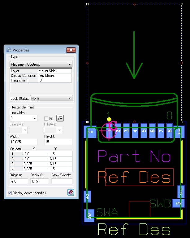
3. The footprint of a component designed for subsequent connection on the board with another component (e.g., a mating connector) near the board’s surface does not reserve the required space for this other component. This raises the possibility that this board area will be occupied by other components in the future, hindering the required connection. Always control the potential surrounding of the component.
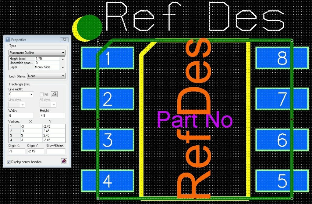
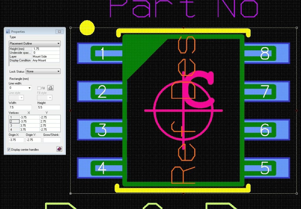
4. The boundaries indicated in the footprint area occupied by the component include only the component’s actual body and the pad areas partially extend beyond this area. This can lead to the automatic design rule check not recognizing the placement of neighboring components as too close. Pads are an integral and non-editable part of the footprint and must fully be within the component’s occupied area.
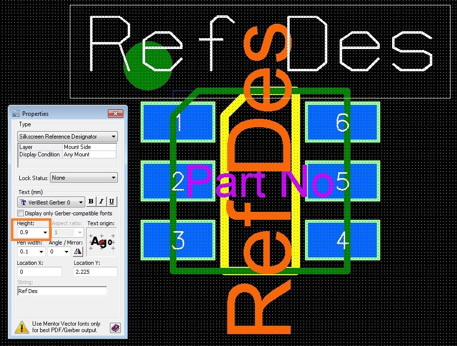
5. When placing textual elements on the silkscreen layer, a font size that is too small is used. Not every PCB manufacturer can provide very fine separate lines in the silkscreen layer. This can result in the paint applied to the board’s surface blending into unreadable blobs instead of clear, legible symbols. You should either rely on the capabilities of your chosen manufacturer or use a font size that any manufacturer can reproduce. Additionally, it should be understood that text in the silkscreen is physically applied to the PCB and cannot be scaled for subsequent reading. It must be legible to the naked eye.
Sintecs has been involved in component library development for 23 years. We have created over 100,000 different components that are successfully used in a wide variety of projects by companies worldwide. If you want access to our ECAD library of electronic components, please write to us at info@sintecs.nl.


