PCB design mistakes; a top 5.
Sintecs professionals know that PCB (printed circuit board) design is a very specific discipline within electronics design. It has it’s own professional path requiring specific education and training. PCB design experience comes with time and through making many designs. We are sharing some of our experience through a top 5 of the most commonly made mistakes while designing PCBs.
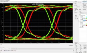
High-speed signal routing errors.
High-speed signals moving through traces give significant emissions. When there is not enough distance between these high-speed traces, emissions interfere with the functionality of the PCB. And result in a malfunctioning circuit. The higher the speed of an interface, especially the flank transitions, the greater the distance required. Using signal analysis tooling shows these interactions in high detail.
Want to know more about these signal integrity (SI) topics?
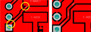
Acute trace angles when entering pads.
When placing traces on a PCB that connect pads and vias, it is very important to connect the traces properly. Do so by connecting pads using a perpendicular angle or to one of its corners. Pieces of copper break off more often when designers do not follow this rule. These pieces can cause short circuits in the PCB, affecting the lifespan and functionality of the final product. Design for manufacturing checks (DFM) can greatly aid in the elimination of these PCB design mistakes.
Want to know more about Design For Manufacturing (DFM) challenges?
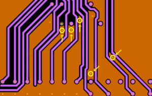
Using a ground plane to fill a signal layer.
Ground planes are often used to fill a signal layer. Designers overlook negative outcomes by doing this. For example:
- Not terminated planes can function as antennas. Solve this by always placing 2 vias in a piece plane.
- Allow the ground to flood around a via if the layout of the PCB easily allows for this.
Prevent amplification of signals by remembering these two simple rules above.
Curious about other PCB layout challenges?
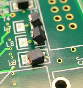
Risk of tombstoning during assembly of small 2 pin parts.
An overlooked issue when placing small 2 pin parts on a PCB is tombstoning. Tombstoning occurs when traces leading towards pads have unequal thickness. Because of the difference in thickness of the copper used in the trace uneven cooling will occur. This causes the thicker side to cool slower than the thin side, then detaching the not yet fixed pin and stands up straight (so-called tombstoning).
Curious about other PCB layout challenges?
Ceramic parts (e.g. capacitors) placed too close to the board’s edge.
When producing new PCBs they are a part of much larger panels. At the end of production you remove the PCB from these larger panels. When removed, by breaking or cutting them, it is possible that little cracks appear (due to mechanical forces). If you place a sensitive ceramic part near a PCB edge, they can damage during the separation process. This damage can result in long term performance loss.
Curious about other PCB layout challenges?
This top 5 PCB design mistakes is just the tip of the iceberg. When it comes to electronics design there are many more challenges to cover. Want to be kept up to date on how Sintecs faces them? Subscribe below:


