Signal Integrity in a nutshell
A simple explanation of the essence of Signal Integrity
We have noticed that signal integrity is an unknown concept. Therefore on this page, we explain broadly what signal integrity means, what negative impact it can have on your high-speed design and how simulations can limit or even prevent this.
A signal integrity analysis and simulation can be performed at different moments in your design process. If your design contains high-speed components, it is definitely recommended. A simulation can be performed, for example, when a customer does not get his prototype working, or only at low speed. Nowadays this is happening a lot more often, since following the design guidelines and rules is no longer adequate.
In addition, we have many customers who use signal integrity simulations even before they start designing. In this way, potential problems are identified and prevented at an early stage.
What is signal integrity?
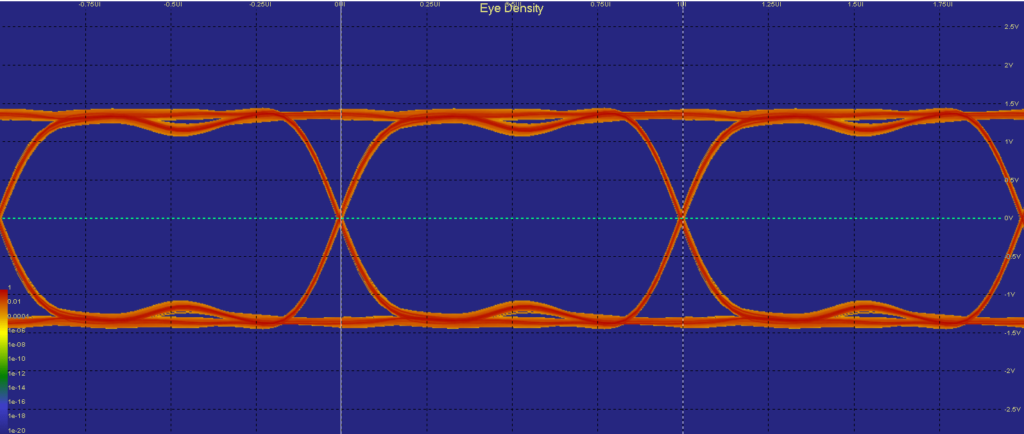
Signals on a Printed Circuit Board (PCB) travel from one electric component to another. When the signal that arrives at a component is not of good quality, the board can become unstable or dysfunctional, especially at higher speeds.
What can go wrong?
If signal integrity is compromised, the signal will be distorted. Effects like overshoot, ringing, switching noise, skew, IR-drop may occur. This will cause functional problems like timing errors, threshold issues, crosstalk, EMI emission, and local hot spots.
These problems are unwanted by-products of complex DDR designs.
What is the cause?
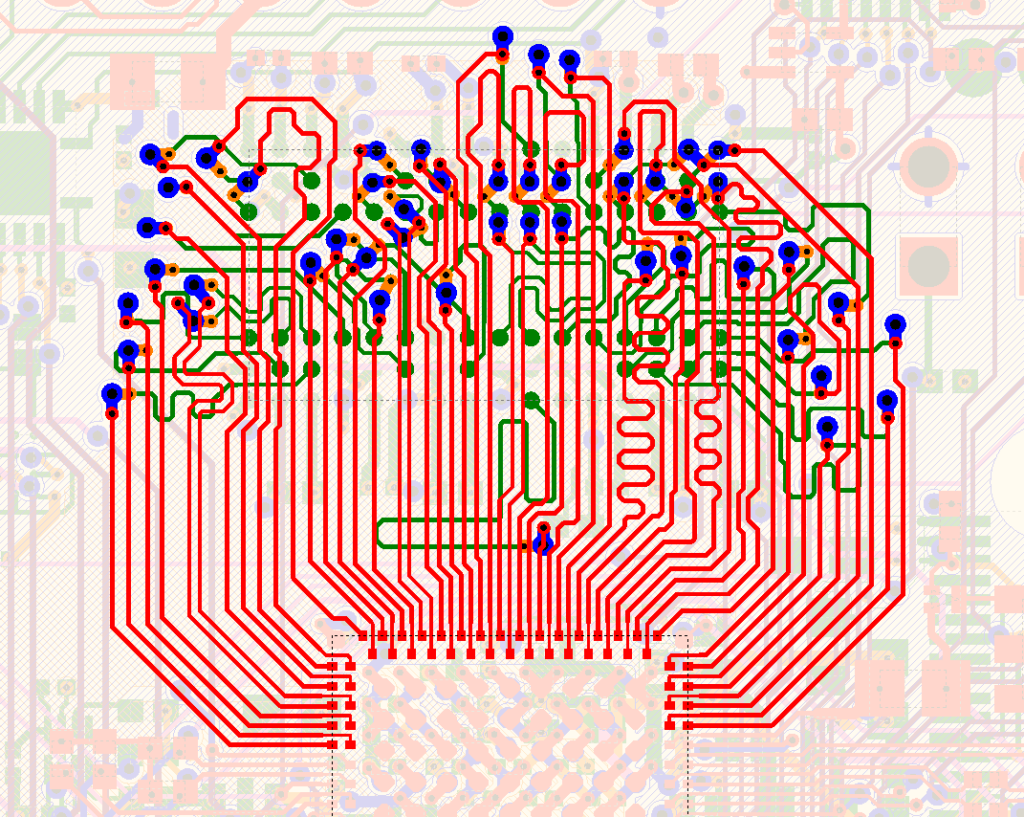
The signal quality does not only depend on the design or PCB routing (interconnect length, characteristic impedance, via usage, delay, decoupling, power distribution network design, etcetera), but also on IC die technology, IC package parasitic effects and wave propagation in dielectric layers.
When does it occur?
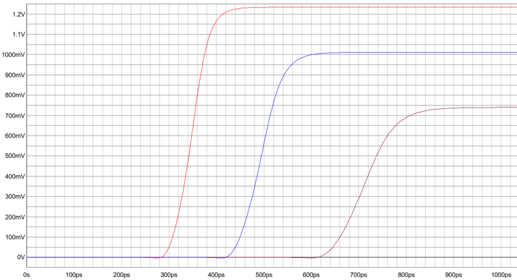
The principles behind signal integrity apply to any electronic design. However signal integrity issues are more likely to cause problems when: data transfer speeds are higher, rise and fall times are faster (die technology), core voltages are lower and thus currents are higher, and interconnect distances are larger (PCB complexity). So beware if you are using a CPU or FPGA (for example from NXP, Xilinx, or Altera) in combination with DDR3, DDR4, PCIe, USB 3.0, SerDes, or Gigabit Ethernet.
What can you do about it?
It is not always enough to design carefully, and layout according to the design rules. Signal integrity simulations or analyses, based on full-wave solver algorithms, will show how signals behave precisely. Next, the layout is modified to fix signal integrity issues, thus increasing the robustness of the design.
Full-wave solver:
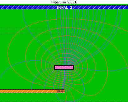
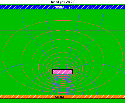
In image 1, a screenshot from Hyperlynx, the interconnect has a partial reference plane which affects the EM fringe fields (partial weak coupling) resulting in lesser signal integrity. In image 2 the interconnect has a full reference plane (full strong coupling) which contributes to much better signal integrity.
What are the benefits of signal integrity analysis?
Pinpointing signal integrity issues in a prototype costs a lot of lab effort, and fixing the issues is not always possible. Performing signal integrity analysis as part of the design saves a lot of trial-and-error, reduces the number of prototype iterations, creates more stable electronics, and decreases time to market.
Our working method for signal integrity simulations
The quality of a signal integrity simulation depends on the quality and the completeness of the models and information that is used. This is why we always recommend our customers to deliver a complete package during the quotation phase. This package must contain simulation models, a PCB stackup, PCB material information, Via information, Power Supply information, and specification and validation parameters.
If the customer is unable to provide the necessary information, generic models are used in order to achieve the best results.
Once the data is received or collected, our analysis engineers can start the analysis in MentorGraphics Hyperlynx. Through our collaboration with Mentor, we actively contribute to optimizing and improving the simulation software.
Collaboration with PCB layout engineers is extremely important before, during or after the execution of a simulation or analysis. Impedance and termination advice can be directly processed in Altium or Xpedition, after which it can be checked again in order to make sure we have not overlooked anything.
Contact us to request a quote or for more information about signal integrity.


