Signal Integrity at low speed
About the importance of Signal Integrity even for a “low speed” design.
Applicable to: Hardware Engineer, PCB Layout Engineer, FPGA Engineer, PCB Architects and more.
Article author: Melvin Mengerink, Signal & Power Integrity Engineer at Sintecs.
Being a ‘hardware’ or layout engineer is a demanding position where a lot of variables and choices are constantly re-considered. These choices require in-depth knowledge of multiple disciplines, including high-speed signaling. Before we can design for high speed we must know what IS high speed. Even a low-frequency signal can have high-speed characteristics.
High speed is based on a reference level, otherwise high or low would have no meaning at all. With my current experience, high speed starts at > 1 GHz, but just before I started doing signal integrity analyses it was > 1 MHz. The difference between those moments is the amount of sheer knowledge I obtained in the last year. But, is it correct to qualify a signal as high speed just by the signal frequency, as seen in Figure 1?
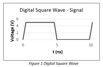
In a perfect digital square waveform there are three main sections: The rising edge, the transition from logic ‘low’ to logic ‘high’, the constant voltages, GND: 0 V / VDD: 5 V and the falling edge, the transition from logic ‘high’ to logic ‘low’. I have taken a signal from 0 V to 5 V as an example. This, of course, depends on the signal created by the buffer drivers (e.g. FPGA).
The rise and fall times of IC components have seen major developments in the last couple of decades which still relates to Moore’s law of increasing transistor count per effective square mm. Smaller transistors make it possible to increase edge rates, thus enabling faster signaling speed. Unfortunately, this also applies to lower speed signals as the edge of modern IC’s remains incredibly fast.
The change between the constant voltages is called the fundamental frequency and can be low speed, e.g. 100MHz. Low speed, in this case, means that transmission line effects do not need immediate attention. But what about the rise and fall times?
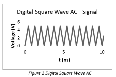
If we look at Figure 2, we see that the AC component of the signal, by stitching the rise and fall times together, is much faster than the original signal. This is the part that behaves and propagates as a wave through the PCB.
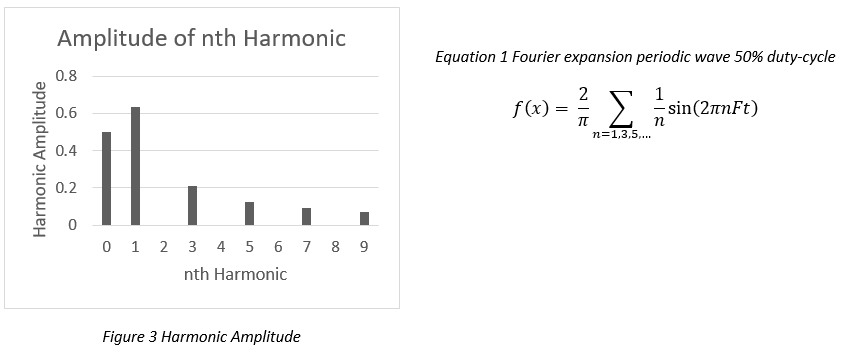
The Fourier expansion of a digital ‘perfect’ square wave is composed of multiple sinusoids. Higher frequencies have a lower magnitude than lower frequencies and will be less ‘visible’ in the minimum and maximum regions of the waveform. The Fourier expansion, to determine the amplitude of the odd harmonics, is shown by equation 1 [Selby, 1973]:
Where n is the harmonic count, F is the frequency and t is the time.
If we would map this out in a graph it would look like Figure 3. We can see that the fundamental frequency (zeroth harmonic) is the average of the square wave (i.e. 0.5 x VDD). It declines rapidly with every odd harmonic. There are no even harmonics in a perfect square wave (duty cycle 50%).
Harmonics up to the 5th or 7th, sometimes even 9th, are usually considered in digital waveforms. You can see in figure 3 that the amplitude difference between the 7th and 9th is negligible. By not considering higher harmonics a bit of simulation accuracy is lost and reflections that are masked by this frequency will not be found. The lower amplitude of these harmonics will rarely cause any threshold violations. Including the harmonics into your design means that a proper signal transmission would require the consideration of 700 MHz, or 900 MHz signals, in lieu of the original 100 MHz signal frequency.
In order to make the call that a signal, or signal’s edge must comply to signal integrity regulations, one must first calculate the time delay of the signal, equation 2 [Hall and McCall, 2000]:
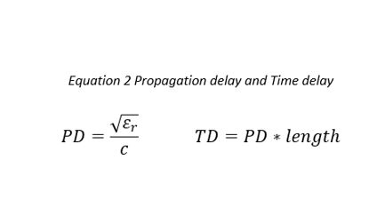
Where PD is the propagation delay, TD is the time delay, εr is the dielectric constant of the PCB or enclosing material and c is the speed of light. Epsilon r (dielectric constant) should be multiplied by the mu r (permeability), but including this variable makes the approximation a lot more difficult, so the permeability of air (=1) is chosen to simplify, meaning there are no magnetic materials in the vicinity.
The energy or EM waves, created by, e.g. a logic ‘low’ to a logic ‘high’ transition, is guided by the copper of the interconnect, meaning the ‘wave’ itself travels in the dielectric material. This material determines the maximum ‘speed’ (or propagation delay) of the signal. The trace geometry including the length of the interconnect determines the time delay. Therefore, the length is a critical parameter to sweep during the design.
If the time delay is bigger than or equal to 20% of the rise or fall time, signal integrity is relevant and the interconnect (trace) is considered a transmission line. This can and probably will result in inter-symbol interference (ISI) and reflections if not designed properly. If the propagating signal has already traveled forth (to the load) and back (to the source) before the next transition starts the interconnect is not considered a transmission line.
Final word:
Do not underestimate the importance of signal integrity simulations and analysis. Even in a 133MHz signaling QSPI-bus, serious signal integrity issues have been found. In this article, I have shown that even low-frequency signals created by modern IC’s can have fast edges resulting in unintended transmission lines. Many of these issues are intermittent and very expensive to solve after the hardware is ordered.


