3 core recommendations for making schematic symbols
A schematic symbol is a part of a library component that represents the component as a part of the electrical circuit. Unlike the part of the library component that represents it on the printed circuit board (called a “cell”, or “footprint”), the schematic symbol is always shown conventionally, without regard to the actual size and physical characteristics of the component. The schematic symbol should represent the function performed by the component and show the possibilities for electrical connections with other components and electrical circuits.
Through this article we would like to share with you 3 useful recommendations on how to develop a schematic symbol that would be anticipated as a professional one by any skilled engineer:
1. Clearly depict all pins present on the component in the symbols. Avoid hidden and discarded pins, even if they are not used. This helps to avoid unnecessary errors and reduces the number of questions from schematic designers while creating a scheme.

2. We have encountered many times the schematic symbols where pins were arranged in numerical order one after another. This is not the best practice, as it greatly hinders the further work of the schematic designer, while the job of the librarian should be to facilitate this work.
Therefore it is highly desirable for qualified librarians to familiarize themselves with the basics of schematic technique, in order to start understanding the functioning of specific blocks and pins of a component and arrange the pins in a way that makes the schematics of the developed device more logical.
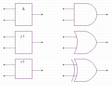
In our library, we group and arrange pins according to their operational relationship or by their shared function, if there is one such. See the incorrect and accurate examples below.


3. In educational materials, there is one main recommendation for schematics layout: “when developing schematics, it is preferred to direct the signal along the schematic drawing from left to right and/or from top to bottom“. It is obvious that this recommendation is also applicable to each individual schematic symbol. Component input pins should be located on the left side of the symbols, outputs should be on the right side of the symbols. Bi-directional pins, and pins intended for connecting passive elements may be located more freely.

Still, there are many situations when it is convenient and reasonable to ignore the practice of “inputs on the left, outputs on the right” on the level of specific schematic symbols. For example:
3.1 When a component serves as a divider between two different parts of the scheme (galvanically separated areas, areas with different signal levels, etc.). Component’s pins related to different sub-circuits should be placed on different sides of the symbol, despite the fact that each side will have its own inputs and outputs:

3.2 When a component is a mediator in the control chain, between the control area of the scheme and the controlled area. Similarly to the previous example, it is advisable to place the pins directed to the control part and the pins directed to the controlled part on different sides of the symbol. In this case, the control part of the scheme is assumed to be located on the left (source of control information), and operated – on the right (consumer of control information), the direction of information transfer is from left to right.
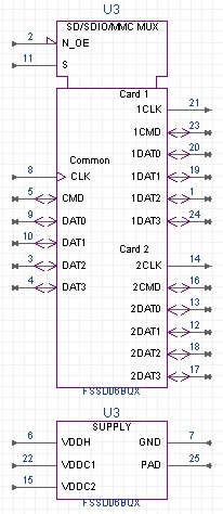
3.4 If a component contains several groups of closely related pins, such as multiple interfaces of the same or different types or multi-digit buses. To improve the readability of the scheme, it is necessary to keep the pins of the group together. If you follow the rule “inputs on the left, outputs on the right,” each group will require an area of the symbol on both the left and right sides, which means placing the groups one under another. As a result, the symbol usually becomes excessively tall. At the same time, each interface is usually connected to a specific area of the scheme with all its pins, and it is inconvenient to have part of these pins on the left and part on the right of the symbol. Therefore it may be more practical and understandable to keep the entire group of inputs and outputs of one interface together on one side of the symbol, depending on the convenience of layout or other secondary factors.

In conclusion, we would like to remind you about the two most important prerequisites defining the general look of a schematic symbol.
A. There are only two main approaches for representing schematic symbols (conveniently called American and European). In general, there is no fundamental difference between them, the “European” style is a descendant of the “American” style. The presence of different styles should be taken into account when working with datasheets of different origins, and for a single project or for every single central database of components it is advisable to choose only one of the styles and stick to it.

B. Since symbols represent their functions conditionally, each company can invent and use its own system of conventions. Problems arise when an interaction between different companies or engineering groups is required, each of which has its own conventions. To resolve this problem, standards for the depiction of schematic elements have been developed and published. These standards are not mandatory, only advisory. However, if each of the communicating parties adheres to similar recommendations in their own schemes, the probability of incorrect mutual understanding is greatly reduced. Familiarization with these standards is very useful for specialists in developing library components. Before “inventing” something that you have not used before, we advise you to check the standard, it is likely that it contains ready-made recommendations that will be understandable to “outside” specialists.
Within the present article, we have suggested only a few basic preferences for high-quality schematic symbols. A corporate guidebook for library development may have hundreds of pages full of specific technical requirements. So oftentimes developing schematic symbols and PCB footprints becomes a complex discipline that has to be performed by well-prepared engineers.
Sintecs has a team of educated engineers performing ECAD library development upon request professionally and efficiently. Contact us to get more details about the service.


